- AI infrastructure
- Semiconductors
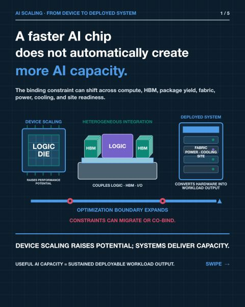
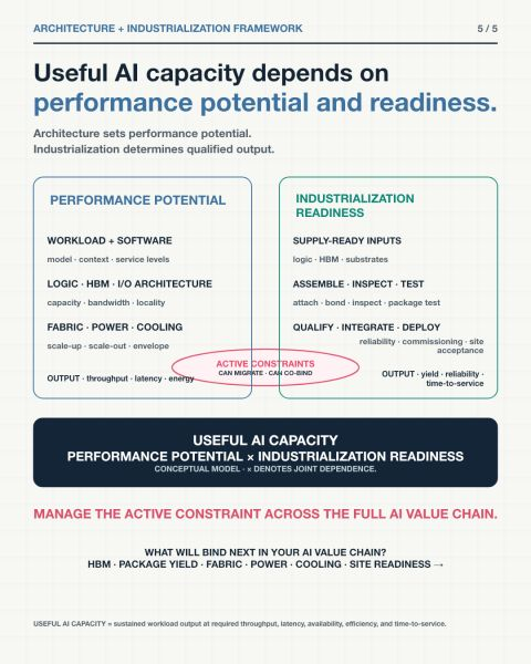
A faster AI chip does not automatically create more useful AI capacity.
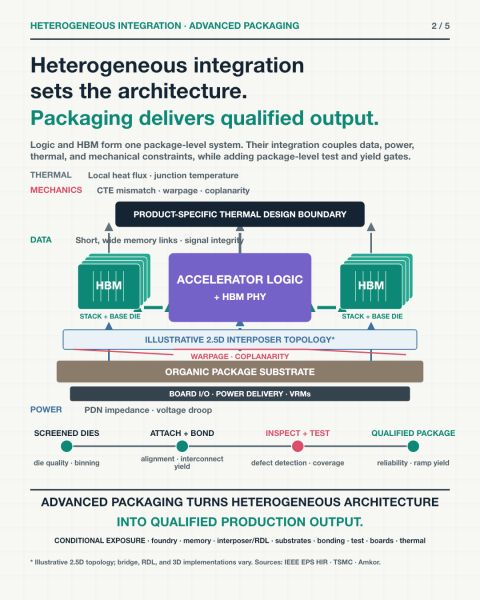
The binding constraint is increasingly system-level, and it can migrate or co-bind.Device scaling raises performance potential. But translating that potential into sustained, deployable workload output requires co-optimization across heterogeneous integration, HBM, advanced packaging, fabric, power delivery, cooling, test, qualification, and site readiness.
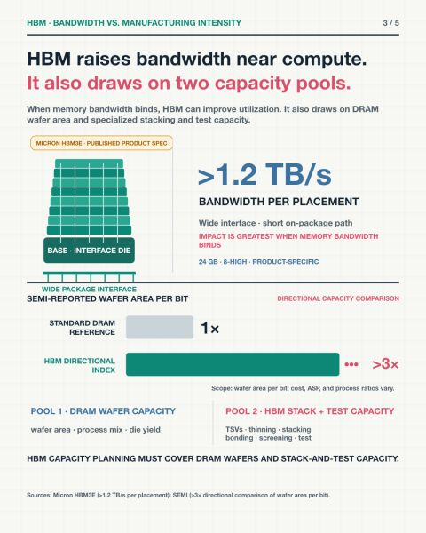
HBM illustrates the point. It can materially improve accelerator utilization when memory bandwidth is the bottleneck. Yet HBM also draws on at least two specialized capacity pools: DRAM wafer area and HBM stack integration, including TSV formation, thinning, stacking, bonding, screening, and test. HBM planning is therefore more than a conventional memory-volume question.
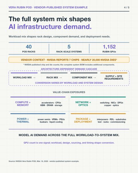
At the system level, the GPU count is only one signal. Workload mix shapes rack design; rack design shapes component demand; and that demand propagates with varying magnitudes and timelines across compute, memory, networking, optics, power semiconductors, cooling, packaging, and deployment infrastructure.
My takeaway: manage AI capacity as a joint architecture-and-industrialization problem, not simply as a chip-output problem.
The question is no longer only, “How many GPUs?”
It is: what will bind next HBM, package yield, fabric, power, cooling, or site readiness?
#Semiconductors #AIInfrastructure #HBM #AdvancedPackaging #HeterogeneousIntegration #ValueChain